From Bare PCB to Functional Assembly: Mastering Surface Mount Technology
A printed circuit board is only half the story. Once the copper traces are etched and the solder mask applied, the board must come to life with hundreds—or thousands—of components. That transformation relies on Surface Mount Technology (SMT), a highly automated process that places tiny resistors, capacitors, integrated circuits, and connectors directly onto the PCB surface, creating a compact, reliable, and high‑performance electronic assembly.
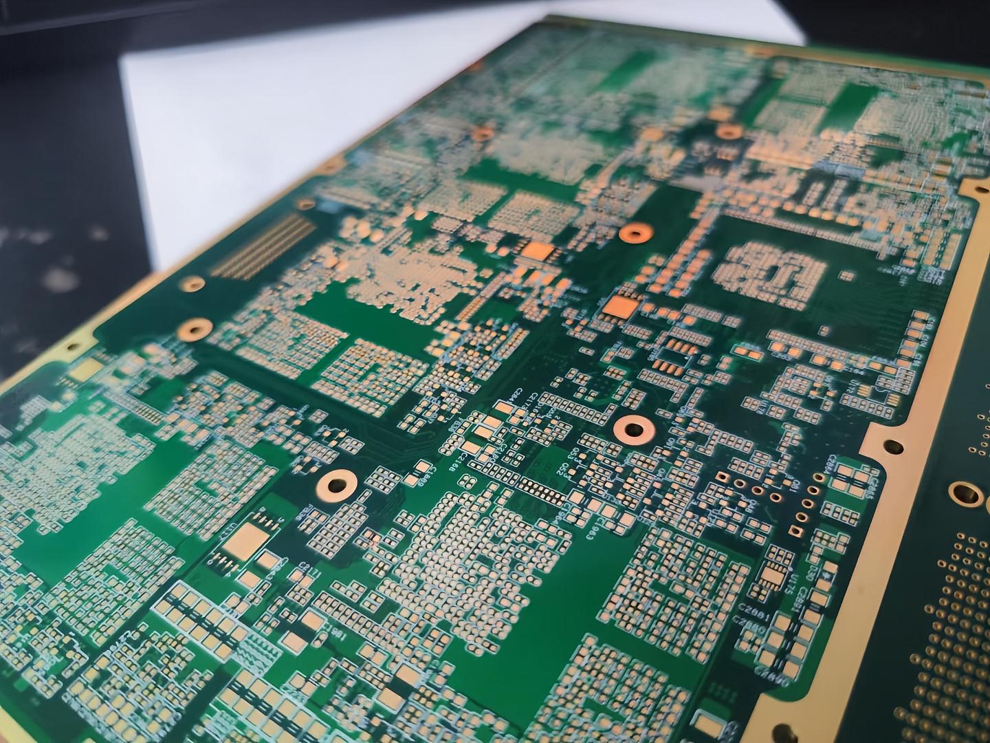
Why SMT Became the Industry Standard
Before SMT became mainstream, through‑hole technology dominated electronics manufacturing. Components had long leads that passed through holes in the PCB and were soldered on the opposite side. While still used for connectors or high‑power parts, through‑hole assembly limits component density and requires more board space. SMT, by contrast, allows components to be mounted on the same side as the traces, enabling double‑sided placement, finer pitches, and drastically reduced parasitics—critical for high‑speed and RF designs.
Today, 01005 imperial (0.4 mm × 0.2 mm) passive components and ball‑grid arrays (BGAs) with 0.3 mm pitch are routinely assembled using SMT, pushing the boundaries of miniaturization. At TOP XINYU Technology, SMT lines are calibrated to handle everything from ultra‑fine‑pitch QFNs to large‑body FPGAs with thousands of solder joints.
The SMT Process Step by Step
- Solder Paste Printing: A stainless steel stencil, laser‑cut to match the PCB pad layout, is aligned over the board. Solder paste (a mixture of tiny solder spheres and flux) is spread across the stencil, depositing precise amounts onto each pad.
- Solder Paste Inspection (SPI): An automated optical system checks paste volume, height, and alignment. Statistical process control prevents printing defects that would otherwise lead to shorts or opens.
- Pick‑and‑Place: High‑speed placement machines pick components from reels or trays and place them onto the solder‑pasted pads. Modern machines can place over 100,000 components per hour with placement accuracy of ±25 µm or better.
- Pre‑Reflow AOI: An optional check verifies component presence and orientation before the board enters the oven.
- Reflow Soldering: The PCB passes through a nitrogen‑atmosphere reflow oven with multiple temperature zones. The precise thermal profile melts the solder particles, forming reliable metallurgical joints as the board cools.
- Post‑Reflow AOI & X‑ray: Automatic optical inspection checks for tombstoning, bridging, and missing components. For BGAs and hidden joints, X‑ray inspection verifies solder ball integrity and void levels.
- Conformal Coating & Final QA: Depending on application, a protective coating may be applied, and the board undergoes in‑circuit or functional testing before shipment.
Materials and Process Control
SMT quality depends on far more than just machines. Solder paste selection (no‑clean, water‑soluble, or rosin‑based flux), stencil technology (nano‑coatings, step stencils for fine‑pitch and tall components), and reflow profiling are tightly intertwined. A poorly optimized profile can cause head‑in‑pillow defects or voiding. TOP XINYU uses real‑time thermal profilers and nitrogen reflow to minimize oxidation and achieve shiny, reliable solder joints—even with challenging lead‑free alloys such as SAC305.
Beyond Prototype: Volume Assembly and Consistency
Whether it's a 5‑board quick‑turn prototype or a 10,000‑unit industrial IoT production run, consistency is everything. SMT demands rigorous environmental controls (temperature and humidity), ESD‑safe handling, and component traceability. Every reel and tray is logged into the Manufacturing Execution System (MES), enabling full traceability from incoming goods to final shipping.
For customers who require mixed assembly (SMT plus through‑hole), selective wave soldering or hand‑soldering cells complement the automated line. This hybrid approach is common in power supplies, automotive modules, and hi‑rel aerospace boards where large connectors or transformers coexist with fine‑pitch SMT components.
The Smart Factory Advantage
Industry 4.0 has reshaped PCB assembly. At TOP XINYU, real‑time data from SPI, placement machines, and AOI systems flows into a central dashboard. Process engineers can then detect trends, adjust parameters, and predict maintenance needs before a defect occurs. This data‑driven approach reduces waste, shortens lead times, and ensures every shipped board meets IPC‑A‑610 Class 2 or Class 3 criteria—the global benchmark for electronic assembly acceptability.
In an era where electronics are embedded in everything from medical wearables to autonomous driving systems, the line between PCB fabricator and assembly partner has blurred. A fully integrated PCB + SMT supply chain, like the one offered by TOP XINYU Technology, simplifies sourcing, ensures traceability, and accelerates time‑to‑market. Because in the end, a perfect PCB means nothing unless every component is placed and soldered with equal precision.