The Backbone of Modern Electronics: A Deep Dive into PCB Technology
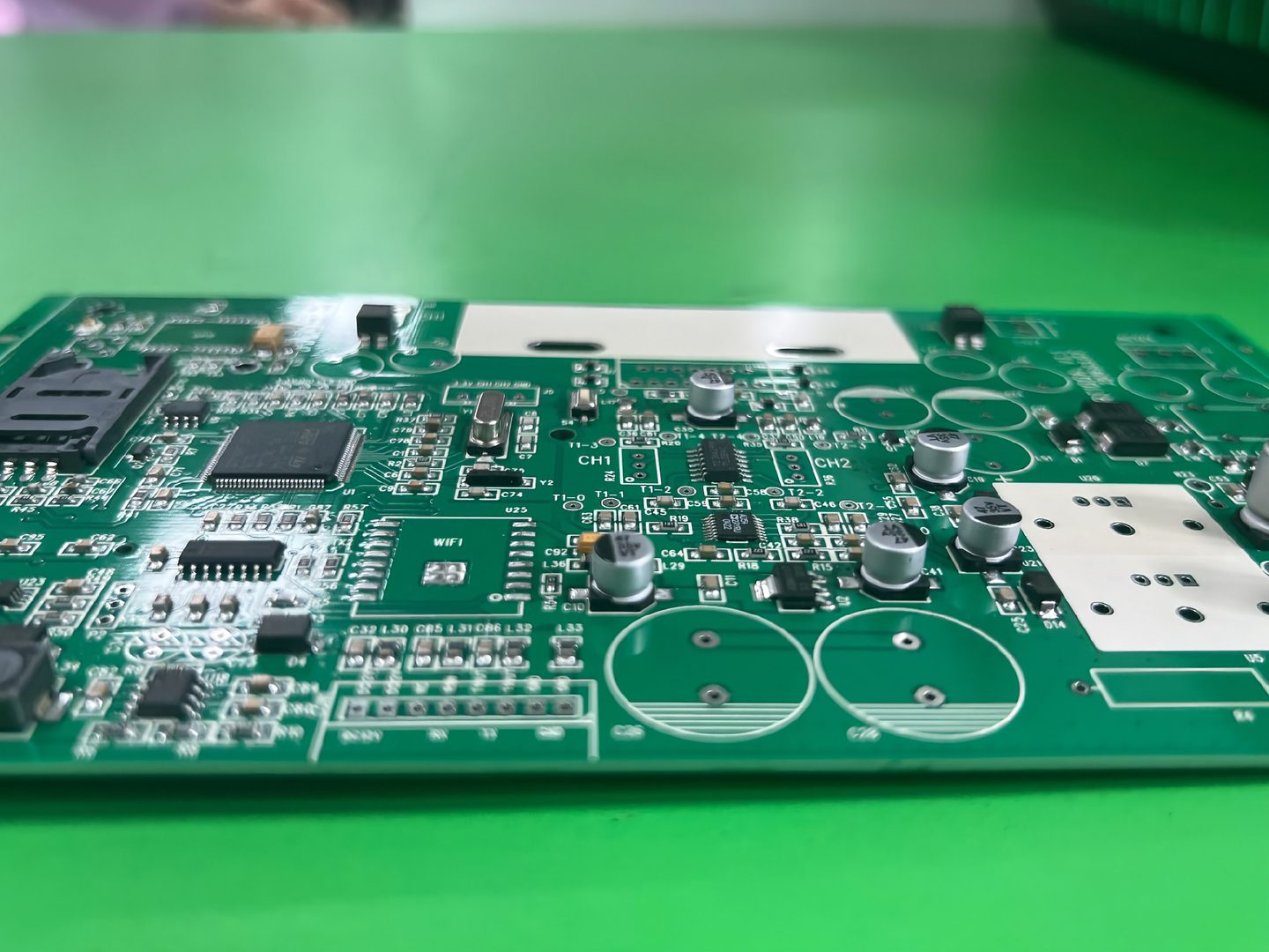
Inside every smartphone, laptop, electric vehicle, and industrial controller lies a flat, often green board covered with tiny components and intricate metal traces—the Printed Circuit Board (PCB). If the chip is the “brain” of an electronic system, the PCB is its skeleton and neural network, providing mechanical support, electrical connectivity, thermal management, and signal integrity. Without high‑quality PCBs, even the most advanced silicon would remain a pile of useless components.
What Exactly Is a PCB?
A PCB is a laminated sandwich of conductive copper layers and insulating dielectric substrates. The most common base material is FR‑4, a glass‑reinforced epoxy laminate that balances cost, durability, and electrical performance. For high‑frequency applications like 5G base stations or radar, specialist materials such as Rogers RO4000 series or Megtron 6 are used due to their low dielectric loss. When thermal performance is critical—think high‑power LEDs or motor drives—aluminum‑core PCBs efficiently draw heat away from components.
The copper foil on each layer is patterned using photolithography and etching to create the required circuit traces. Copper thickness is measured in ounces per square foot; 1 oz copper (35 µm) is typical for signal layers, while power planes might use 2 oz or even 3 oz for minimum voltage drop. Connections between layers are made through plated through‑holes (PTH), blind vias, and buried vias, with via‑in‑pad and back‑drilling techniques employed in high‑speed designs to eliminate signal stubs.
From Design to Physical Board: The Manufacturing Journey
PCB fabrication is a multi‑step process that demands precision and strict process control:
- Design & CAM Engineering: Designers provide Gerber files, and a CAM engineer performs a Design for Manufacturability (DFM) check, identifying potential issues like acid traps, insufficient clearances, or impedance mismatches.
- Inner Layer Imaging & Etching: A dry‑film photoresist is applied to the copper‑clad laminate, exposed to UV light through a photomask, and developed. The unprotected copper is etched away, leaving the circuit pattern.
- Layer Alignment & Lamination: Inner layers are stacked with prepreg (pre‑impregnated bonding sheets) between them, precisely aligned using registration pins, and then laminated under heat and pressure to form a monolithic board.
- Drilling & Plating: Mechanical or laser drilling creates holes for vias and component leads. The holes are then plated with electroless copper followed by electrolytic copper to establish conductivity between layers.
- Outer Layer Patterning & Solder Mask: The outer layers are patterned similarly to the inner layers. A solder mask (typically green, but also available in white, blue, red, or black) is applied to insulate traces and prevent solder bridging.
- Surface Finish: To protect exposed copper pads and ensure solderability, a surface finish is applied—options include HASL (Hot Air Solder Leveling), ENIG (Electroless Nickel Immersion Gold), or Immersion Silver. ENIG is favoured for fine‑pitch components due to its flatness.
- Silkscreen & Testing: A silkscreen layer prints component designators and logos. Every board then undergoes electrical testing—flying probe or bed‑of‑nails—to verify continuity and isolation, followed by visual inspection and sometimes cross‑section analysis.
Types of PCBs and Their Applications
PCBs come in a variety of forms tailored to specific needs:
- Single‑ & Double‑Layer PCBs: The simplest constructions, used in consumer electronics, toys, and simple control circuits.
- Multilayer PCBs: From 4‑layer up to 30+ layers, these handle complex routing in servers, telecommunications, and aerospace systems where dense interconnect and controlled impedance are essential.
- Flexible PCBs (Flex): Built on polyimide or polyester film, they can bend and fold, enabling wearable devices, medical endoscopes, and laptop hinge connections.
- Rigid‑Flex PCBs: A hybrid of rigid and flex technologies, eliminating connectors and increasing reliability in automotive sensors, military equipment, and portable medical instruments.
- Aluminum & Metal‑Core PCBs: Designed for superior heat dissipation in LED lighting, power supplies, and motor controllers.
- High‑Frequency & RF PCBs: Utilize low‑loss dielectrics and precise impedance control for RF amplifiers, antennas, and radar systems up to millimeter‑wave frequencies.
Why Quality Matters
A poorly fabricated PCB can lead to intermittent failures, signal degradation, or complete device malfunction. Key quality indicators include copper‑plating uniformity, impedance tolerance (often within ±5%), solder mask alignment, and the absence of voids in via fill. Advanced processes like via‑in‑pad with planarization, back‑drilling to remove via stubs in high‑speed traces, and X‑ray inspection of BGA joints are hallmarks of a world‑class PCB manufacturer.
At TOP XINYU Technology, these principles guide every project—from quick‑turn 4‑layer prototypes to complex 10‑layer automotive rigid‑flex boards. By combining engineering expertise, rigorous DFM review, and a comprehensive supply chain, the company ensures that every PCB meets the demands of both innovation and reliability. Whether you are launching a startup wearable or scaling up an industrial IoT gateway, the quality of your PCB is the foundation of your product’s success.
The Future of PCB Technology
As electronics shrink and data rates explode, PCB technology continues to evolve. HDI (High‑Density Interconnect) boards with microvias and via‑in‑pad allow for thousands of connections in a square centimeter. Embedded components (resistors, capacitors, and even ICs) within the laminate stack further reduce footprint. Additive manufacturing and 3D‑printed electronics are opening new design possibilities. In this rapidly advancing landscape, partnering with a technology‑driven fabricator that stays at the forefront of these trends is more critical than ever.
In short, the PCB is far more than a simple commodity—it is a precision‑engineered component that defines the performance envelope of modern electronics.