Beyond the Schematic: Optimizing PCB Design for Manufacturability and Reliability
A perfect schematic does not guarantee a flawless physical board. The journey from circuit diagram to high‑yield production involves a meticulous PCB layout phase, where every trace, via, and copper pour directly influences signal integrity, thermal performance, and long‑term reliability. Whether you're designing a high‑speed digital interface, a sensitive analog front‑end, or a dense HDI smartphone motherboard, optimizing the PCB layout is the most critical engineering step between concept and reality.
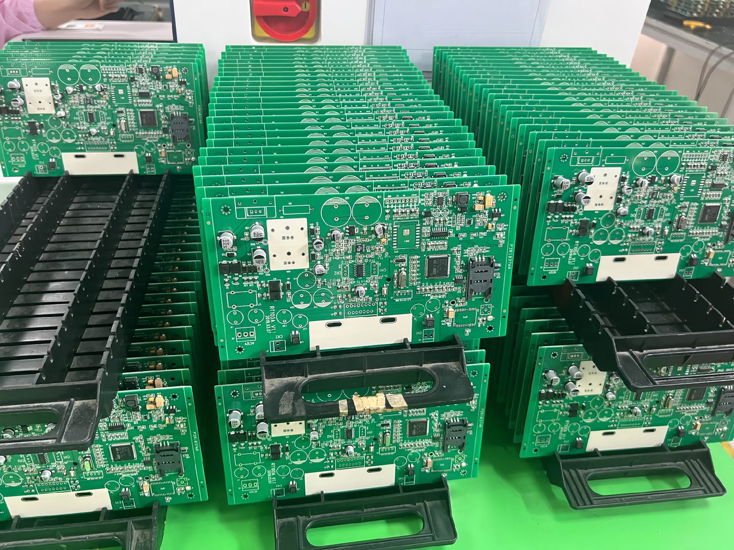
Start with the Stackup: The Foundation of Performance
The layer stackup is often treated as an afterthought, yet it dictates impedance control, crosstalk, and electromagnetic compatibility. A well‑planned 4‑layer stack might use SIG‑GND‑PWR‑SIG, providing solid reference planes and low‑inductance power distribution. For high‑speed designs, 6‑layer or 8‑layer stacks with multiple ground planes and tightly coupled differential pairs become essential. At TOP XINYU, engineers collaborate with customers to define dielectric thicknesses, prepreg materials, and copper weights that match target impedances—typically 50 Ω single‑ended and 100 Ω differential—before a single trace is routed.
For RF and microwave applications above 6 GHz, low‑Dk/low‑Df materials such as Rogers 4350B or Megtron 6 are necessary. The laminate selection impacts not only signal loss but also phase stability and temperature coefficient, critical for phased‑array antennas or automotive radar.
Critical Layout Practices for Signal Integrity
- Controlled Impedance Routing: Trace width and spacing are calculated based on the stackup to maintain constant impedance. Tools like polar Si9000 are used to verify values before Gerber generation.
- Differential Pair Symmetry: High‑speed USB, PCIe, and HDMI lanes require matched lengths and constant spacing to avoid skew and mode conversion. Length matching is performed within a few mils.
- Via Stub Mitigation: In high‑speed links, unused portions of through‑hole vias act as resonant stubs. Back‑drilling removes these stubs, while blind vias or via‑in‑pad techniques eliminate them entirely.
- Return Path Integrity: Every signal has a return current. Gaps in the reference plane beneath a high‑speed trace force return currents to loop, causing EMI and signal degradation. Careful placement of stitching capacitors or vias avoids this pitfall.
Power Integrity: The Silent Foundation
Digital ICs demand clean, stable power rails even as they switch at gigahertz speeds. Power Distribution Network (PDN) design involves placing decoupling capacitors close to IC power pins, selecting appropriate values to cover a broad frequency range (e.g., 100 nF + 10 µF + bulk capacitance), and using thick power planes or wide polygons to minimize DC resistance. Simulation tools like Ansys SIwave or Cadence Sigrity help visualize voltage ripple and target impedance, but even without simulation, following rules of thumb—such as minimizing PDN inductance by using multiple vias to plane—significantly improves reliability.
Thermal Management in PCB Layout
With processors, FPGAs, and GaN power transistors dissipating tens of watts, thermal design is inseparable from layout. Thermal vias under hot components conduct heat to a copper plane or an aluminum core. Copper pours act as heat spreaders; making them larger than the component footprint enhances convection. For extreme cases, embedded coin or metal‑core PCBs are employed. TOP XINYU’s design reviews flag thermally stressed areas early, suggesting component placement adjustments to avoid hot spots and improve long‑term reliability.
Design for Manufacturing (DFM): From Layout to Production
Even an electrically perfect layout can fail in production if DFM rules are ignored. Minimum trace/space, annular ring sizes, solder mask slivers, and acid traps are all checked by the CAM engineer before fabrication. For assembly, pad geometries must match the solder paste stencil design; too large a pad leads to tombstoning of small passives, while too small causes opens. Fiducial marks (at least three) are placed for automated optical alignment, and tooling holes or rails may be needed for panelization.
At TOP XINYU Technology, a thorough DFM report accompanies every prototype order. Designers receive specific recommendations to improve yield, reduce cost, and avoid common errors—making the difference between a board that merely “works in the lab” and one that thrives in volume production.
Prototype Validation and Iteration
After layout sign‑off and fabrication, the very first boards must undergo rigorous testing: time‑domain reflectometry (TDR) for impedance verification, eye‑diagram analysis for high‑speed links, and thermal cycling for reliability assessment. Any deviations feed back into the layout for quick‑turn revisions. With TOP XINYU’s rapid prototyping service, design‑to‑test cycles shrink from weeks to days, enabling agile hardware development in the age of IoT and 5G.
Ultimately, PCB design is an interdisciplinary craft blending electrical engineering, materials science, and manufacturing know‑how. By mastering these principles and partnering with a knowledgeable fabricator, innovators can bring complex electronics to market faster and with confidence.